
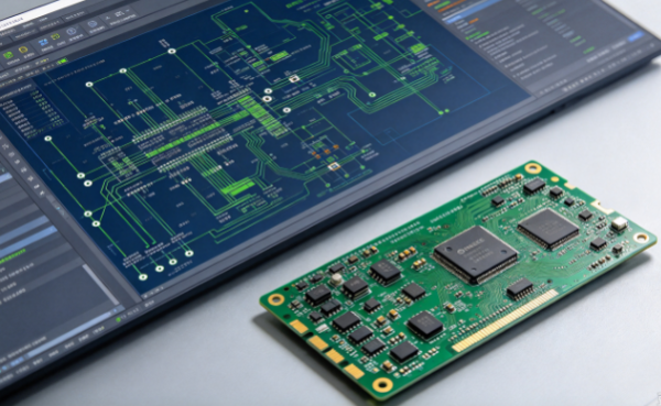
PCB Design
Professional PCB layout & design services for prototype and mass manufacturing, supporting multi-layer, high-speed and HDI circuit boards
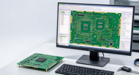
PCB Design Capabilities
Our design team collaborates closely with manufacturing engineers to deliver manufacturable, cost-effective and reliable PCB designs. From rough concepts or schematics to full turnkey development, we provide production-ready design packages for PCB fabrication and assembly.
Supported by senior engineers, we manage the full development cycle: schematic capture, layout, simulation, DFM/DFA review and mass production handover.
We use Altium, Cadence Allegro and Mentor Xpedition for high-speed, HDI, rigid-flex, RF and multilayer boards, focusing on signal integrity, power delivery and thermal management.
Since our designs feed directly into our own production line, we optimize manufacturability from the start, cutting revisions, speeding time-to-market and lowering overall project costs.
Design Parameters
✅ Layer Count: 2–20+ layers
✅ Board Size: Min 5mm × 5mm, Max 1200mm × 600mm
✅ Design Types: Rigid PCB, Flexible PCB, Rigid-Flex PCB, HDI PCB, High-speed & RF PCB
✅ EDA Software: Altium Designer, Cadence Allegro, Mentor Xpedition, PADS
✅ Special Analysis: SI (Signal Integrity), PI (Power Integrity), Thermal Simulation, Impedance Control
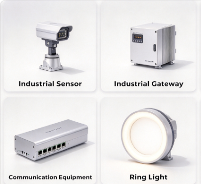
✅ Application Fields: Consumer Electronics, Industrial Control, Automotive, Medical, IoT
What We Need To Start Your PCB Design
✅ Product function & performance requirements
✅ Target board dimension & layer stack-up
✅ BOM list & component datasheets
✅ Special requirements: impedance, thermal, IP protection
✅ Mechanical outline / enclosure drawing
Our PCB Design Deliverables
🟢Gerber manufacturing files
🟢 BOM & CPL pick-and-place files
🟢IPC netlist for verification
🟢 Stack-up & impedance report
🟢 SI / PI / thermal simulation reports
🟢 Source design files (Altium / Cadence / Mentor)
Frequently Asked Questions
Q: What PCB board types can your design team handle?
A: We design rigid PCB, flexible PCB, rigid-flex PCB, HDI PCB, high-speed and RF PCB. Layer count ranges from 2 to 20+ layers, supporting small boards starting at 5mm×5mm up to large 1200mm×600mm panels.
What EDA software platforms do your PCB engineers work with?
A: Our team uses Altium Designer, Cadence Allegro, Mentor Xpedition and PADS. We can import your source files and deliver design outputs compatible with these tools.
Q: What materials or information do I need to provide to start a PCB design project?
A: To kick off your project, please share product function & performance requirements, target board dimension and layer stack-up, plus BOM list and component datasheets. If you only have a concept, we can also start from your specification.
Q: What files will I receive after PCB design is completed?
A: We deliver full manufacturing packages including Gerber files, BOM & CPL pick-and-place files, and IPC netlist for verification. All files are ready for PCB fabrication and PCBA assembly.
Q: What special analysis can you do during PCB layout?
A: We provide signal integrity (SI), power integrity (PI) and thermal analysis for high-speed & high-power boards. Combined with DFM/DFA review, our designs are optimized for manufacturability and stable performance.